Research highlight: "Low-Temperature Atomic Layer Deposition of MoS2 Films" conducted at EPIC, SPID, and KECK-II
Abstract
Wet chemical screening reveals the very high reactivity of Mo(NMe2)4 with H2S for the low-temperature synthesis of MoS2. This observation motivated an investigation of Mo(NMe2)4 as a volatile precursor for the atomic layer deposition (ALD) of MoS2 thin films. Herein we report that Mo(NMe2)4 enables MoS2 film growth at record low temperatures—as low as 60 °C. The as-deposited films are amorphous but can be readily crystallized by annealing. Importantly, the low ALD growth temperature is compatible with photolithographic and lift-off patterning for the straightforward fabrication of diverse device structures.
 |
 |
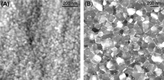
Left: AFM topographic images (SPID) of A) as-deposited and B) annealed MoS2 films.
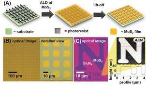
Right: Figure A outlines the process flow for lift-off. A resist was patterned by either maskless photolithography or electron-beam lithography (EPIC). Next, 10 nm of MoS2 was grown by ALD at 80 °C, and the resist was then removed with the appropriate solvent. Photolithography yields uniform arrays of MoS2 patterns across the ca. 1 cm2 sample (Figure B), showing the reliability of the deposition and patterning processes. Figure C : Optical and AFM micrographs and AFM profile (bottom) of MoS2 letters on Si/Si3N4 patterned by electron-beam lithography.
The full article can be found here.