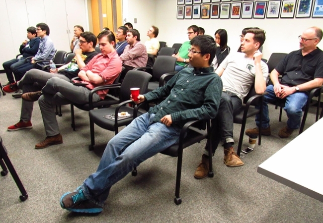
Dr. Hee Joon Jung presents on "TEM Studies on Energy Conversion Materials"

Dr. Hee Joon Jung a, postdoctoral fellow from Pacific Northwest National Laboratory, gave a presentation entitled "TEM Studies on Energy Conversion Materials". Dr. Jung was a candidate for the AC/TEM postdoctoral position with the NUANCE Center/ EPIC Facility. Approximately 30 people attended the talk.
ABSTRACT:
The world’s growing energy needs with sustainable environment will involve not one but a harmonious collection of efficient energy conversion technologies that will work in concert to produce, store, and use the large amounts of energy that humans will soon demand such as solar cell, solid oxide fuel cell (SOFC), and photoelectrochemical (PEC) cell and etc. To provide a scientific establishment for high-efficiency, cost-effective energy technologies, recent research activities have been focused on manipulation of materials at the nanometer scale to increase efficiency of energy conversion devices and exploitation of fundamental advances in charge transport, light absorption, and reaction thermodynamics and kinetics to improve performance of energy conversion devices. To achieve these goals, we need to understand how nano-structuring modifies and governs the properties of materials, and how to control dimensionality and confinement to learn insights. Transmission Electron Microscopy (TEM) with additional advanced functions enables us to apprehend the fundamental relationship between chemical / electronic / optical properties of materials and origin (crystal structure, composition, size, shape) of them through the characterization at atomic and nano/micro scale.
For photovoltaics, 3D generation solar cell using quantum dot (QD) for bandgap tuning will be presented, because semiconductor QDs allow for manipulation of the bandgap position and energy levels of electrons at sub-10nm length scales through control of material chemistry, size, and shape. Atomic layer deposition (ALD) is used to fabricate QDs on high-aspect-ratio nanostructures, as demonstrated by the uniform coating of Si nanowire (NW) array with a single layer of PbS quantum dots and QD/NW composites (US patented) show a blue shift when QD size is decreased, suggesting a route to fabricate unique 3-D nanostructured solar cell or photoelectrochemical (PEC) cell for water splitting. In particular, anisotropic shape such as dome-shaped QD leads to local bandgap variation within a single QD, as demonstrated by a series of individual, electrically isolated, dome-shaped PbS QDs using monochromated 80kV scanning transmission electron microscope-valence electron energy loss spectroscopy (STEM-VEELS). The fact that consistent increase in the localized bandgap from the lateral center of the QD towards the edges, which is attributed purely to shape, tells us that not only size control at the nm scale but also shape control can be used to tune the bandgap of QDs. NiSi NWs for back contract (US patented) and controlled direction growth of ZnO NWs, giving only 1%reflection of light due to light trapping, would provide additional benefit. Graphene formation from SiC by laser ablation and Mg-implanted SiC (Eg=2.38~3.26 eV) deliver higher conductivity and stable electronic device operation to ~900 °C. Multitasking LaCrO3/STO perovskite structure, 2-D Nb-dopedMoS2 film (p-type) and 0-DMoS2 QDs would allow for unique opportunity for new optoelectronic devices. These approach may open significant pathways towards the miniaturization and enhancement of a wide range of solid-state devices that rely on electron dynamics.
For SOFC, low temperature operation (< 500 °C) with high power density over 1 W/cm2 enables commercialization (Prinz group achieved 1.3 W/cm2 at 450 °C corrugated YSZ/YDC bilayer in 2013) and understanding of grain boundary (GB) is essential to enhance SOFC performance because GB has been known for highway for oxygen ions through cathode-electrolyte-anode, but had not yet been proven directly. Before we achieved it, we had been researching GB condition and role from diverse materials such as Ga-doped CeO2 (GDC), Ba-doped YSZ (BYZ), and YSZ and it turns out that GB is positively charged due to charge balance between dopant segregation and oxygen depletion confirmed by STEM-EDS/EELS map, Kalvin Probe Microscopy (KPM), Negative Cs-corrected TEM imaging and simulation in different papers. However, because this ex-situ experiment provided only indirect implication of GB at non-operating condition, in-situ gas TEM experiment on CeO2 under H2 gas at 700 °C was introduced using eels of Ce M5/M4 peak ratio to check Ce oxidation state. The fact that Ce3+ concentration is increased at GB than grain under SOFC anode operating condition verifies that positively space-charged GB leads accumulation of excess electrons at GB causing reduction of Ce4+ to Ce3+, implying that GB is significantly active reducing site of O2 which allows drastic O ion movement through GBs. And recent 3D YSZ nano-tubular structure will be presented.
