Features
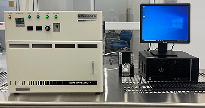
Thin film stress originates from the lattice mismatch between the film material and the substrate. Stress caused from deposition to a wafer can be tensile (the film is stretched to fit the substrate and causes the edges of the wafer to curl upward) or compressive (the film is larger than the substrate and causes the wafer edges to bow downwards). The Toho FLX-2320S, thin film stress measurement instrument determines the stress on the substrate by comparing the curvature before and after deposition. A laser scanner is used to measure the radius of curvature. The stress of the thin film can then be calculated mathematically.
- Measurement Range: 1×10⁷ to 4×10¹⁰ dyne/cm2
- Temperature Range: Room temperature to 500 oC
- Substrate Diameter: From 1” to 8” (4” and 6” recommended)
- Two solid state lasers for optimal signal readout from a large variety of films: a class IIIa laser with 4 mW power and 670 nm wavelength, and a class IIIb laser with 4mW power and 750 nm wavelength.
- Minimum scan step: 0.02 mm
- Inert gas: N2, flow rate 2-10 CFH. Cooling gas: CDA, flow rate up to 500 CFH.

